Course Project
Problem Statement
Design an 8-bit processor with 3 address format and having Immediate addressing mode.
Processor modules
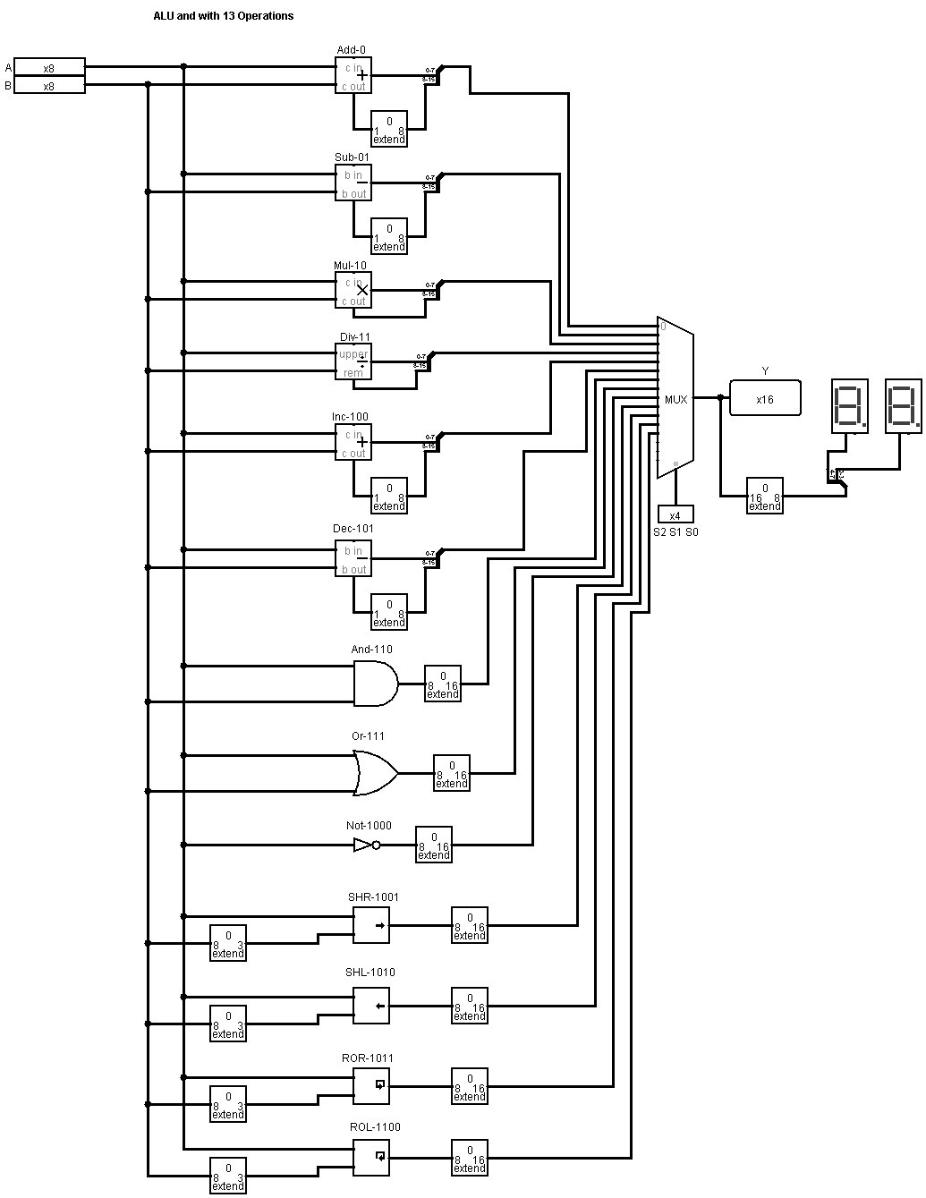
ALU:
An Arithmetic Logic Unit (ALU) is a critical component of a processor that performs arithmetic and logical operations on data. It operates on binary numbers and acts as the computational brain of the CPU. The ALU takes input data, executes operations based on control signals, and provides the result as output.
- Arithmetic Operations: Addition, subtraction, multiplication, division, increment, and decrement.
- Logical Operations: AND, OR, NOT, and similar bitwise functions.
- Shift/Rotate Operations: Shifting or rotating bits to manipulate data efficiently.
Key features of an ALU include:
This specific ALU implements 13 operations: add, sub, mul, div, inc, dec, and, or, not, shr, shl, ror, and rol, making it versatile for performing arithmetic, logical, and bit manipulation tasks.
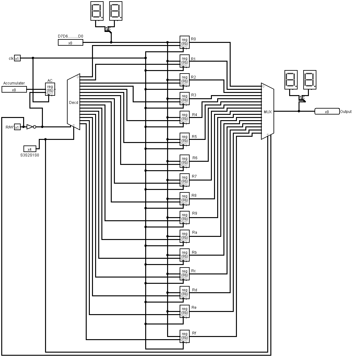
Register Bank:
The register bank consists of 16 8-bit registers (R0 to R15), used for temporarily storing data. A decoder selects a specific register for read or write operations based on control signals, while a multiplexer (MUX) routes the selected register's data to the output. The R/W control determines whether data is written to or read from the registers, and the accumulator temporarily holds data for these operations. A clock signal synchronizes all activities, ensuring efficient and fast data handling within the processor.
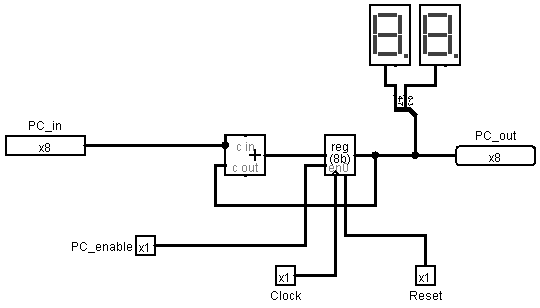
Program Counter:
The program counter (PC) is an 8-bit register that stores the address of the next instruction to be executed. It can load a new address via PC_in, increment automatically to the next address on each clock pulse when PC_enable is active, and reset to a predefined address using the Reset signal. The PC_out provides the current address, while the clock ensures synchronized operation, enabling sequential instruction execution and manual updates when required.
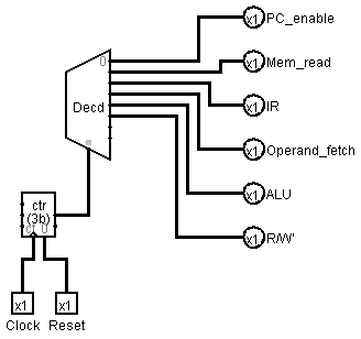
Control Unit:
The Control Unit (CU) is a component of a computer's processor that directs and coordinates all operations by generating control signals. It manages the flow of data between the CPU, memory, and input/output devices, ensuring that instructions are executed in the correct sequence and timing.
- PC_enable: Activates the Program Counter (PC) to send the address of the next instruction to memory.
- Mem_read: Signals the memory to read data or an instruction from the specified address.
- IR: Loads the fetched instruction into the Instruction Register (IR) for decoding and execution.
- Operand_fetch: Fetches the operands required for executing the instruction (from memory or registers).
- ALU: Activates the Arithmetic Logic Unit (ALU) to perform the required arithmetic or logical operation.
- R/W': Indicates whether the operation is a read ('1') or a write ('0') in memory or a register.
Download the Individual files By clicking on the below image names
Integrated processor
Description about Processor
An 8-bit processor is a microprocessor that processes and transfers data in 8-bit chunks. It operates using an 8-bit data bus, making it efficient for small-scale operations like embedded systems and low-power devices.
The processor is designed with:
- 3-Address Format: Allows three operands in instructions (e.g., destination, source1, source2). This improves performance by reducing intermediate steps.
- Immediate Addressing Mode: Data is directly embedded within the instruction, reducing memory access time and enhancing execution speed.
Speciality:
- Efficient for arithmetic and logical operations due to the 8-bit data structure.
- Simplified instruction set for faster development and debugging.
- Ideal for low-power, high-performance tasks in devices like calculators, sensors, and small control systems.
Features:
- Compact Design: Suitable for space-constrained systems.
- Simplified instruction set for faster development and debugging.
- Low Power Consumption: Ensures efficiency for battery-operated devices.
Advantages:
- Speed: Faster operations with immediate data access.
- Simplicity: Easier to program and debug due to straightforward architecture.
- Cost-Effective: Less expensive to design and manufacture.
- Portability: Lightweight and highly adaptable for various applications.
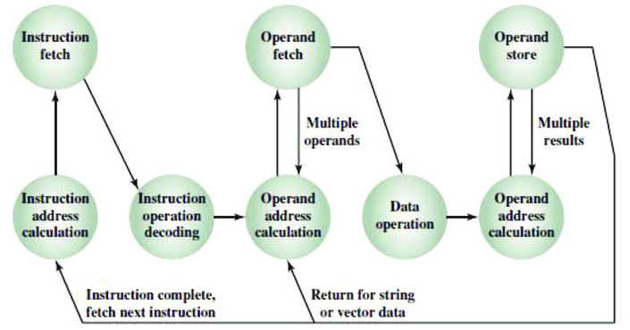
Intruction State Diagram
Microinstructions
- ADD R1, R2, #5 // R2 = A, R1 = 0
- SUB R3, R4, #3 // R4 = 8, R3 = 0
- T1: (MAR) ← (PC)
- T2: MBR ← (MEMORY)
PC ← PC + I - T3: IR ← (MBR)
- T4: R1 ← R2 + 5
- T5: (MAR) ← (PC)
- T6: MBR ← (MEMORY)
PC ← PC + I - T7: IR ← (MBR)
- T8: R3 ← R4 - 3
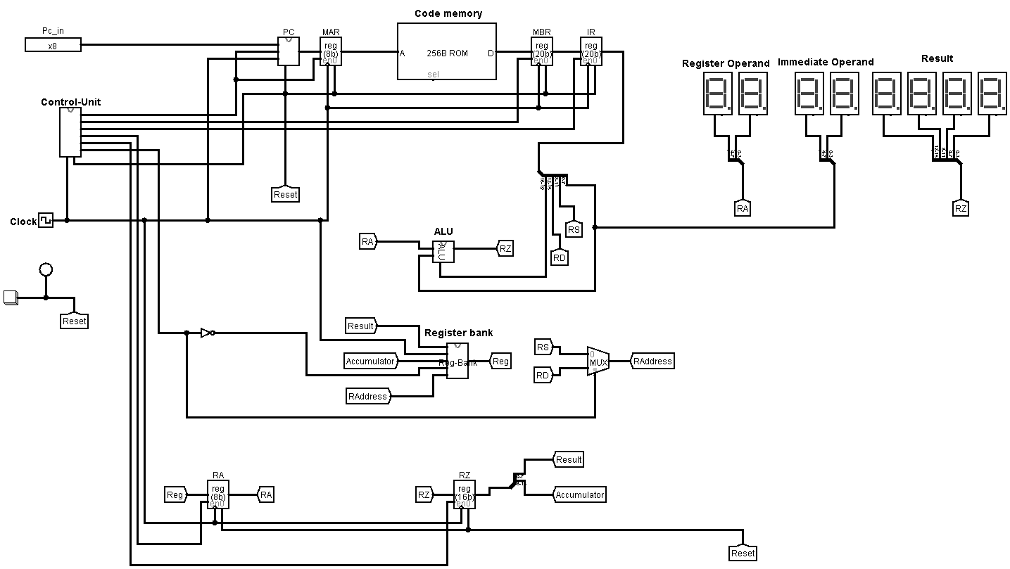
Working of the Processor
1. Fetch Phase:
- Step 1: Program Counter (PC):
- The PC contains the address of the next instruction to execute.
- The address from the PC is loaded into the Memory Address Register (MAR).
- Step 2: Fetch from Memory:
- The instruction at the address in the MAR is fetched from the code memory and loaded into the Memory Buffer Register (MBR).
- Step 3: Update PC:
- The PC is incremented to point to the next instruction in memory.
2. Decode Phase:
- Step 4: Instruction Register (IR):
- The instruction in the Memory Buffer Register (MBR) is moved to the Instruction Register (IR).
- The Control Unit decodes the instruction to identify the operation and operands.
3. Execute Phase:
- Step 5: Operands Fetch:
- The required operands are fetched depending on the instruction type:
- Register Operand: Register values (e.g., R1, R2) are fetched from the register bank.
- Immediate Operand: Immediate values (e.g., #5) are directly extracted from the instruction.
- Step 6: ALU Operation:
- The Arithmetic Logic Unit (ALU) performs the required operation based on the instruction:
- ADD: Adds the values (e.g., R2 + 5) and stores the result in the destination register.
- SUB: Subtracts values (e.g., R4 - 3) and stores the result in the destination register.
- Step 7: Store Result:
- The result of the ALU operation is stored in the destination register or accumulator (e.g., RZ).
Activity learning and challenges
Activity Learnings:
- Designed an 8-bit processor using the 3-address format and Immediate addressing mode.
- Understood how the processor fetches and decodes instructions in a cycle.
- Gained insights into the steps involved in executing each instruction, such as fetching, decoding, and executing.
- Learned about different addressing modes, specifically how Immediate addressing allows using constant values directly in the instruction.
Challenges Faced:
- Handling different instruction formats and ensuring the proper handling of data across registers.
- Managing memory efficiently to store and retrieve data while executing instructions.
- Debugging issues related to the timing of instruction cycles and ensuring proper synchronization.